TL;DR: I am hoping to fix a broken USB drive….
For purely scientific interest, I have been interested in chip decapping for a while. Decapping is slightly archaic because only the larger integrated circuits tend to be made with actual removable caps these days.

Instead, ICs are FAR more commonly cast into epoxy and often glass reinforced epoxy.
There are a couple of destructive ways to decap epoxy chips. Sometimes you can literal just break the package and expose all or part of the silicon die with all the interesting bits therein, but that is really random. You can also use pretty extreme heat to soften the epoxy enough to peel it off the die.
The most effective way, and one which leaves at least a chance that the chip may still operate is to use heated 70% nitric acid to *dissolve* the epoxy. This is really effective and pretty hazardous, so requires good preparation and a not insignificant list of supplies, not the least of which is the 70% nitric acid. As I am writing this, a couple of online sources sell it to individuals for about $50 for a 100ml bottle (a little less that 1/2 cup Imperial) plus a $40 HazMat fee from the shipper. You need borosilicate glass (Pyrex is a brand name of borosilicate glass) because nitric acid will react with regular soda class. There are a lot of YouTube videos on the subject. I may tackle it for scientific purposes in the future, whenever I feel like dropping a hundred bucks on a half cup of evil juice.
What brings this whole subject to light is that a) I have had a physically damaged USB drive for many years and b) I have seen a few videos lately where talented individuals have used a fiber laser to vaporize the epoxy off of an SD card to expose the factory test connections in order to recover data on that card.
Now, I don’t have a spiffy fiber laser, but I do have an xTool D1 that I have been using for a variety of cutting and engraving projects. Surprisingly, as of this writing, the laser does not have it’s own blog category. Must fix.
This USB drive was in a laptop that was dropped. Instantly, it stopped working correctly. It would kinda work, showing a drive letter in Windows, but every attempt to interact with it would produce either an error or a bunch of nothing. For example, drive E: is there, with zero bytes in use, zero bytes available, etc. The card does mount, but there appears to be a disconnect between the controller and the actual storage within the device.
So, disassembly revealed that under all that plastic was a single tiny module, completely potted in epoxy, with a visible crack across it’s width.
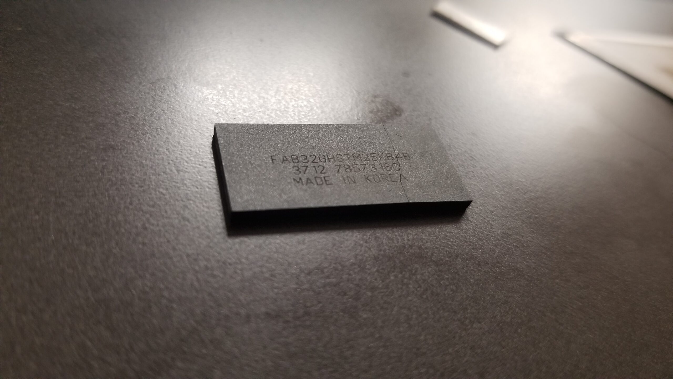
On the other side of this module is the 4 pin USB connector on what is pretty obviously a printed circuit board. I suspect the entire device is a small board with naked chip dies attached and the whole thing potted in epoxy. All the plastic physical packaging is just to position and protect this little module. I should mention that this is a PNY brand device and it’s been long enough that I don’t remember the capacity, but it’s likely a 16MB or maybe 32MB. It’s not big by today’s standards.
This device was dropped quite some time ago, maybe 2012 or so. I think if I ever gain access, I’ll be able to realistically time stamp it, but I’m jumping WAY ahead. During those intervening years, I have occasionally tried to access the data. Mostly, I have tried to reflex the crack enough to make contact with whatever conductors were broken by the crack, which is generally my assumption as to what is broken. Maybe the PC board cracked in the right place to deny power to the storage chips, but not the controller. I don’t recall the specific utilities I used, but at least two of them were able to verify that the controller was responding, but that it could not see the storage.
So, back to the xTool D1. My particular device is a 10W blue diode laser that will cut up to about 10mm thick plywood, but it’s much happier with thinner stuff than that. I have cut everything from copier paper to acrylic to EVA foam and, with a little experimentation with the speed and power settings, it has performed wonderfully.
I didn’t want to just blindly charge into attempting to cut away the epoxy in my lobotomized USB drive, so I found a known dead circuit board and started eroding the epoxy on a couple of it’s onboard chips. I happened to pick the dead wireless link device that I had replaced earlier this year.
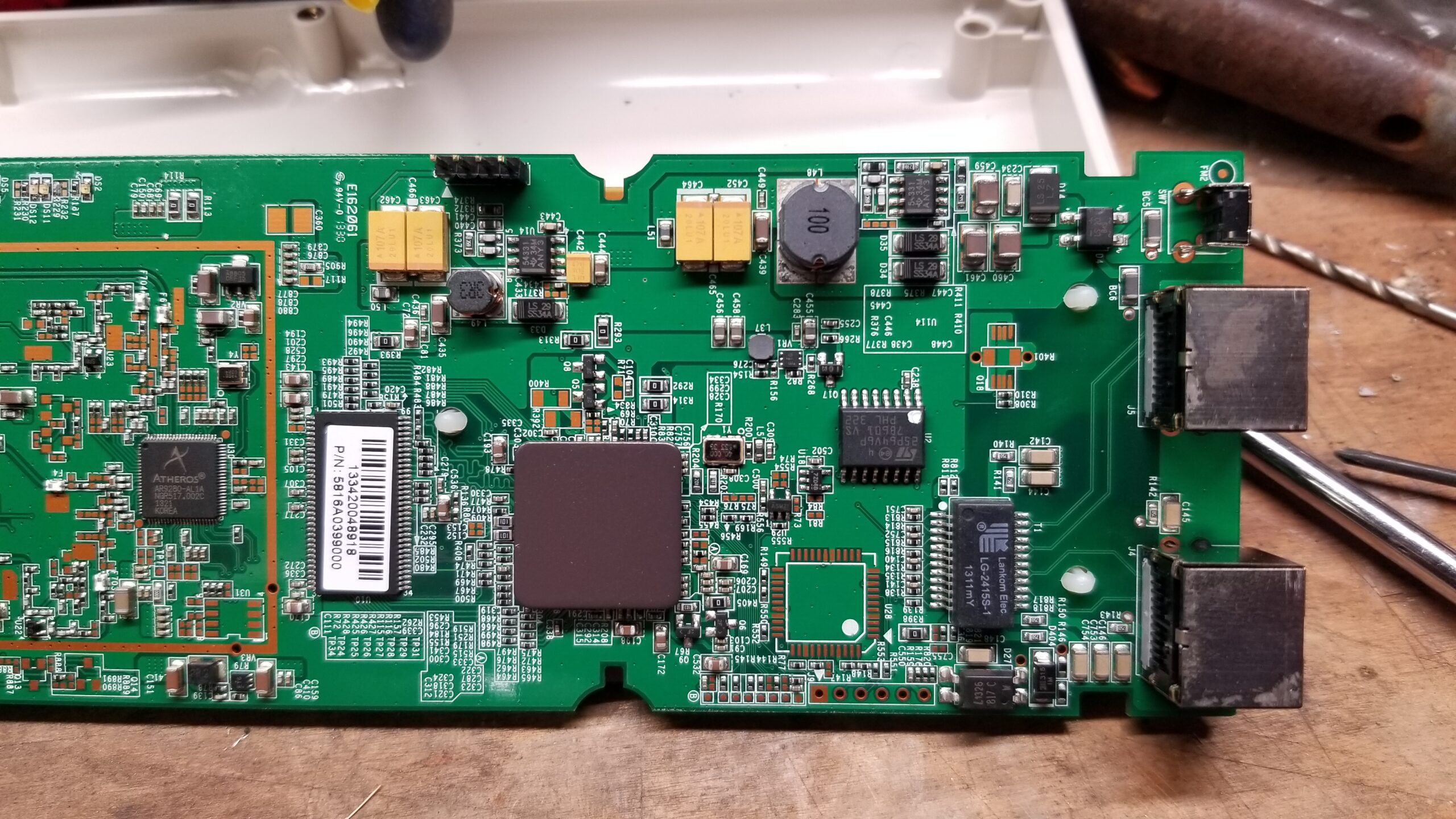
I set the xTool to ‘fill’ a 11mm square and positioned the laser over the left-most chip shown in the picture above. I played with various speed and power settings until I had an idea how it would chew it away.
I am not sure if it is specifically ash or if the laser burns away everything except the glass reinforcement, but a pass or two of the laser leaves a gray/white layer and the laser seems to no longer have much affect. Maybe if I had more than 10 watts to work with, it would be simpler.
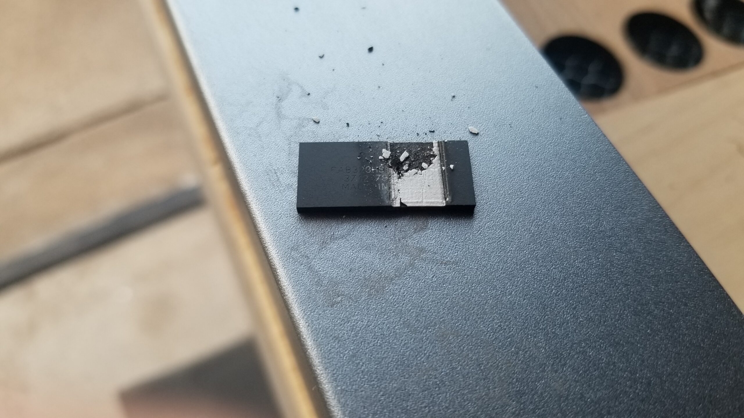
After chipping and scraping away some layers of epoxy off of that chip, I decided that I had nothing left to lose by starting with those settings and seeing how it did with the USB drive module.
For the first pass, of COURSE I didn’t have the chip lined up perfectly, so it left a millimeter or so of chip untouched on the righthand side. I readjusted and ran the fill again. I noticed that the material was less “reactive”, it tended to reflect blue light rather than glow with a bright white burning color. I removed the module and used the corner of a single edge razor blade to chip away the gray/white ash layer.
If I was very careful, I could remove fairly large chips of this ash material. After a couple of passes, it looked like this:
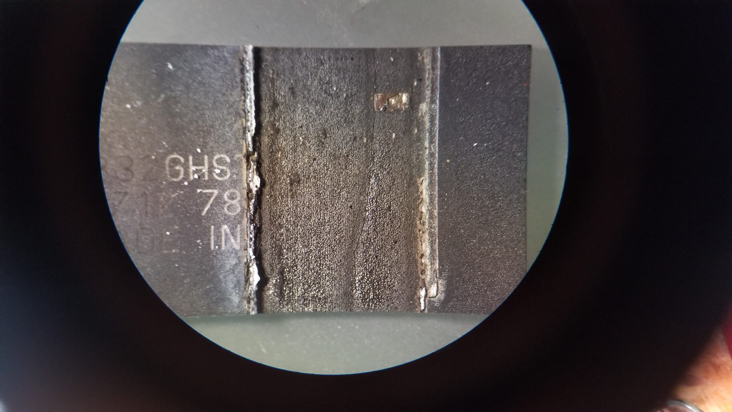
Note a few specifics… I think rectangle in the upper left may be a capacitor being exposed. I hope the laser does not damage it.
Next, edges of the crack seem to erode quicker, leaving a trough that follows the crack. This may be a localized thermal effect.
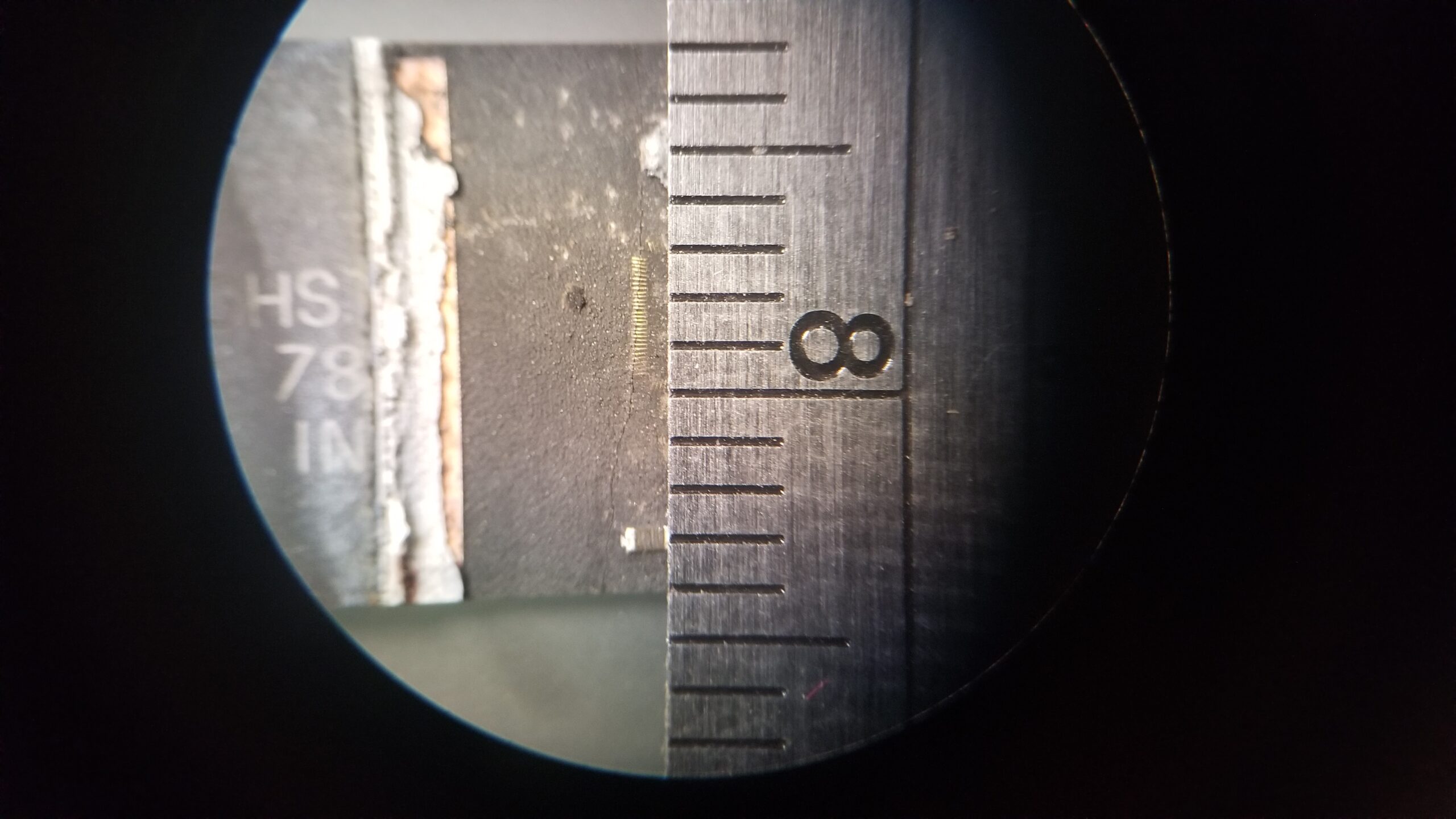
Finally, you can definitely detect the 0.05mm spacing I chose to fill in the pattern. My experiments with the old wireless system chips showed that the default 0.1mm spacing was pretty crude at this level, but it *was* twice as fast to run. 🙂
I ran the pattern a few more times and exposed the mother lode:
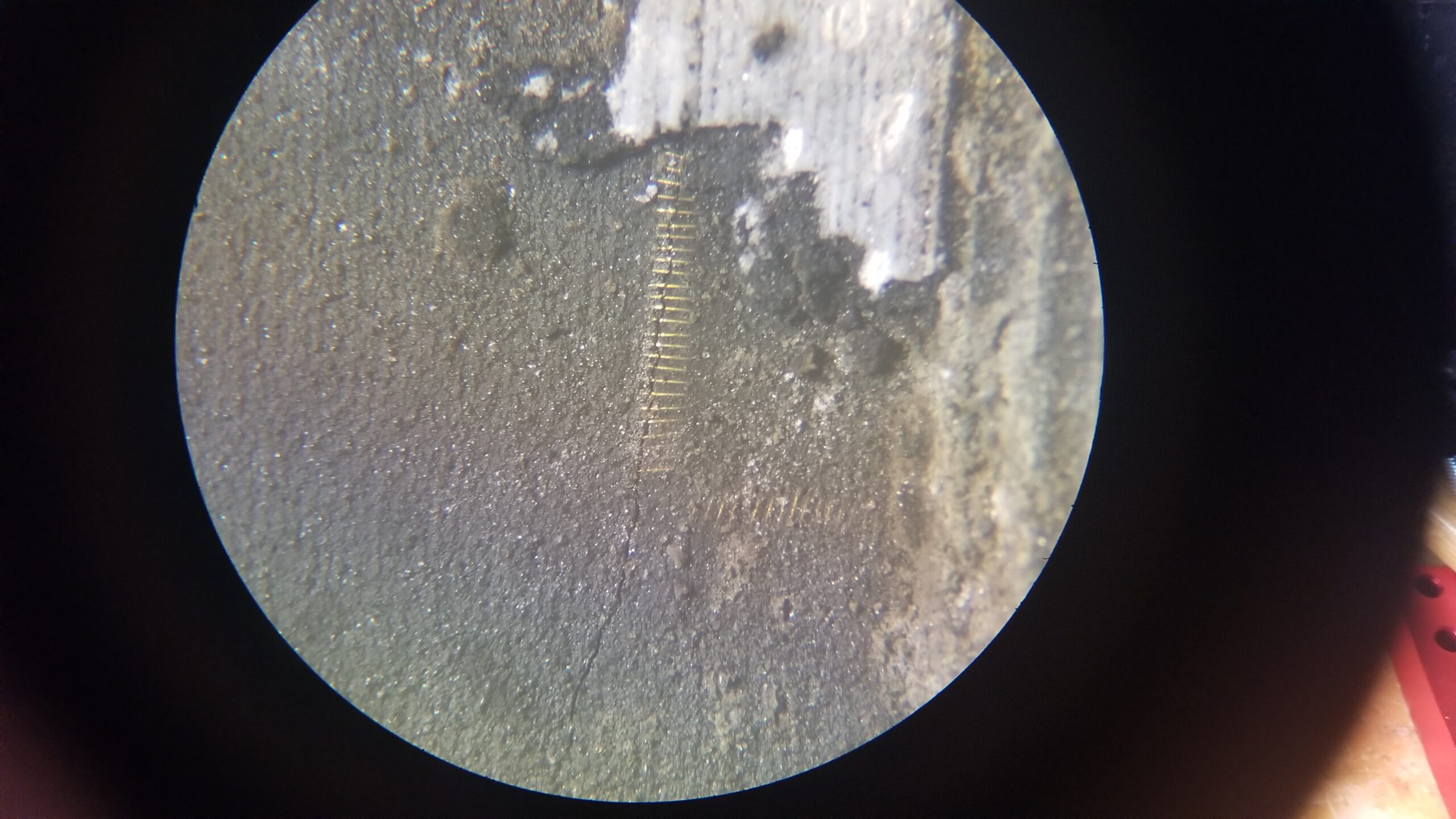
A bundle of bond wires, apparently all broken by the crack in the module.
It is good news because I am now confident I have found the problem. It is bad news because instead of maybe one or two broken power traces on the PC board, I have (I think 29) broken wires that fit roughly into a 3mm space.
I am *planning* to attempt to use fine solder paste and rework gun heat to solder bridge between the broken ends, somehow *not* also bridging the tiny 0.01mm gap between wires. I may make an attempt first to see if it will work at the current depth I have burned away with the laser. If not, I will need to tweak some laser values and try it again….